I
built a flip chip aligner when I was working as a post doc research
associate at the Rutgers University (in 2003). It was planned to use in
the bump boning CVD diamond pixel detectors we were testing to CMMS
pixel readout chips.The main task of the device is to bring a pixel
sensor and a pixel
readout chip together precisely so that bumps on each of them make
contact. Since bumps are usually about 20 microns in size and of about
100 microns in pitch, it is a challenging task.
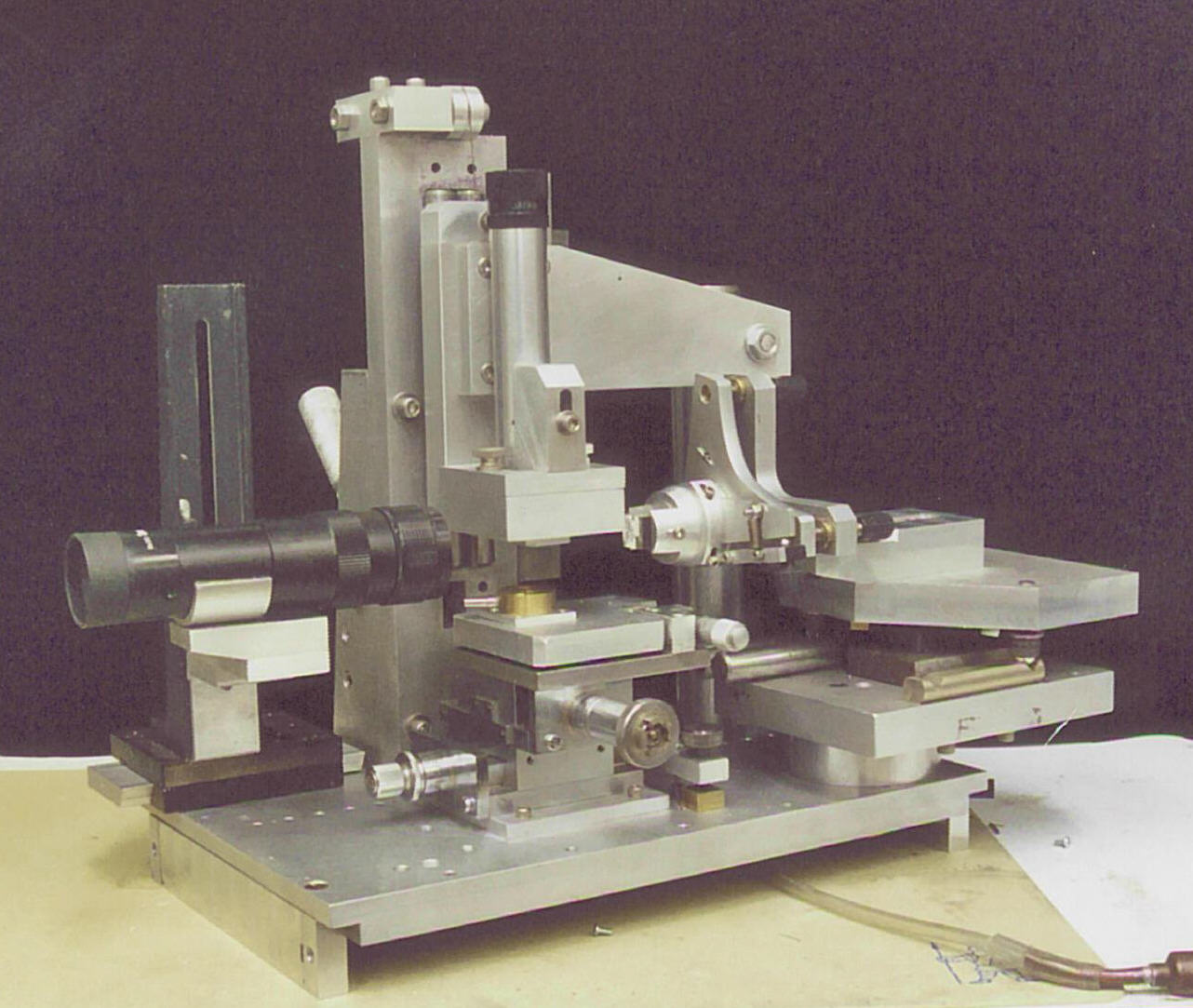
First prototype flip chip aligner
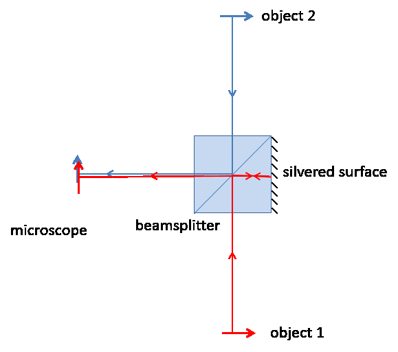
Principal of the optics used in the aligner
Shown above is a photo and the
principal of optics of first prototype to test the concept and
feasibility. It was based on ideas that I developed and
mostly made from scrap metal and parts I machined
myself.
To obtain backlash free linear motion kinematic slides in the form of steel balls sliding on two
metal rods were used. They were
held together by permanent magnets. A beamsplitter with
one of the surfaces silvered is used to view both surfaces
simultaneously. A Beamsplitter was aligned
first looking at a reticles which were known to be aligned correctly. (more pictures)
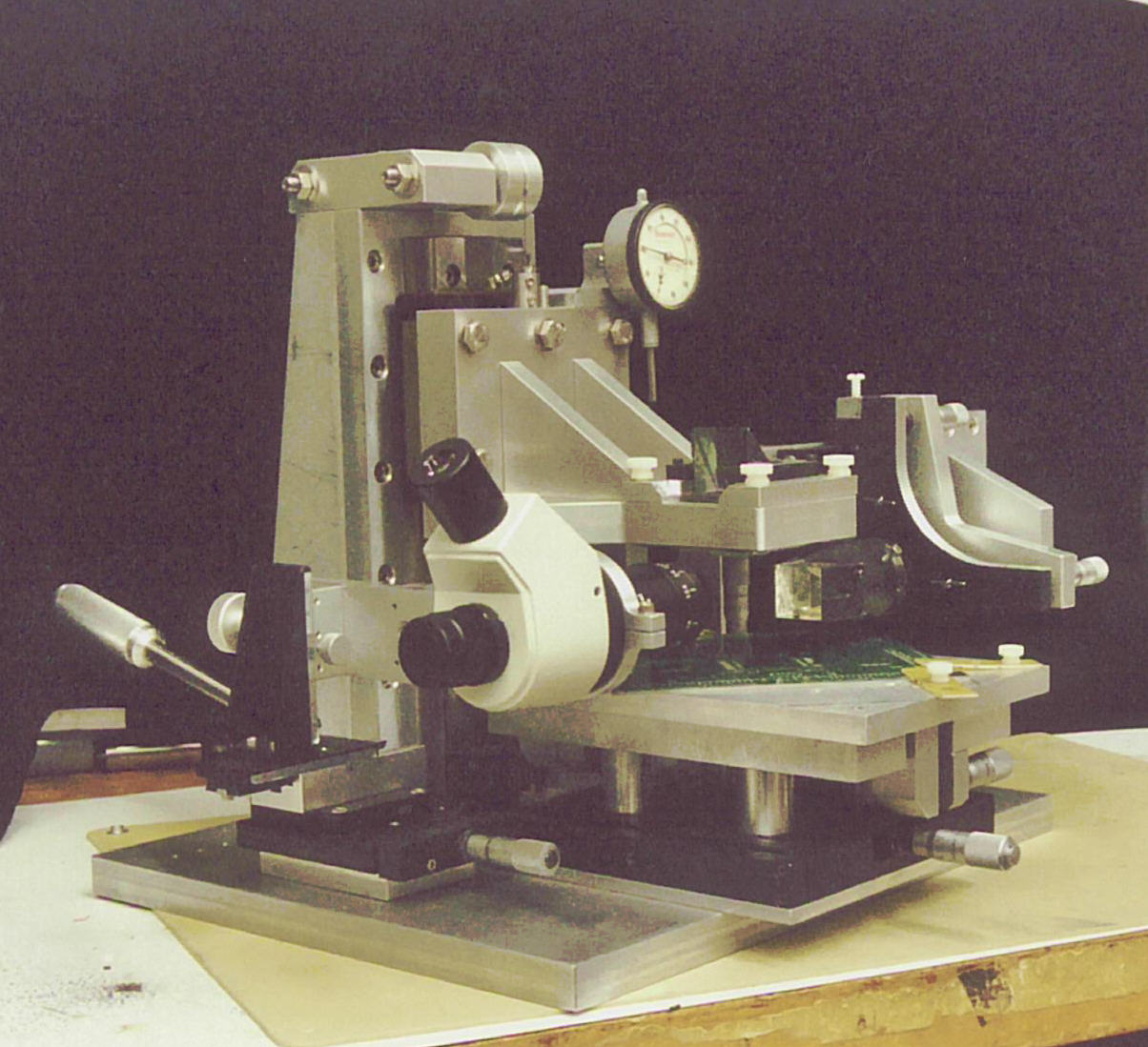
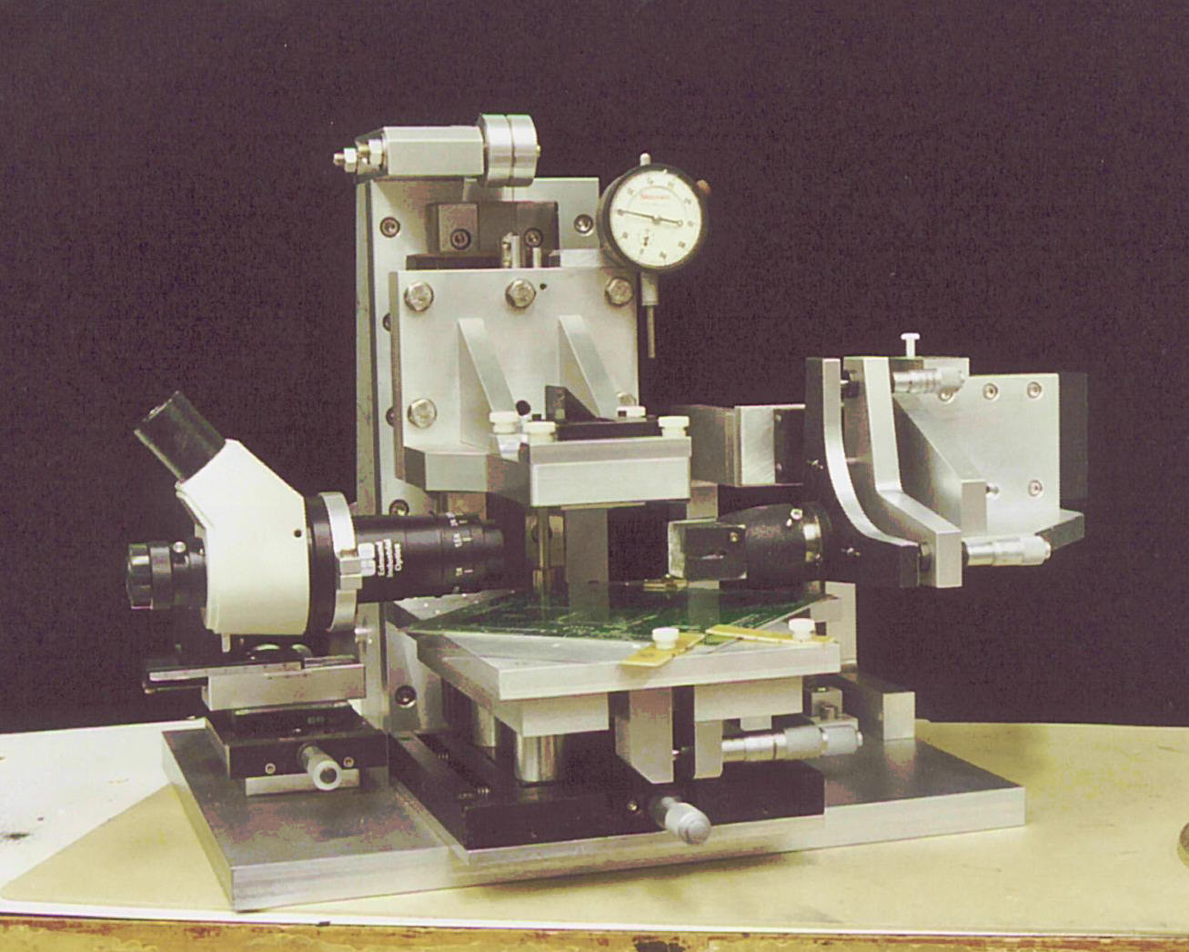
Aligner used to mount fine pitch array FPGAs on printed circuit boards.
Photos above shows an aligner I built to mount ball grid array type FPGAs (for the fabrication
of prototype PCBs for the CMS pixel readout) as well as a learning
exercise for a more precision aligner. It was machined at the physics
department machine shop and used commercial linear bearings. Total
material cost was about $2000. We used it to mount fine pitch pin and ball grid array FPGAs
on the first prototype FPGA-TBM test boards. It also provided valuable
experience for the next version (more pictures)
.
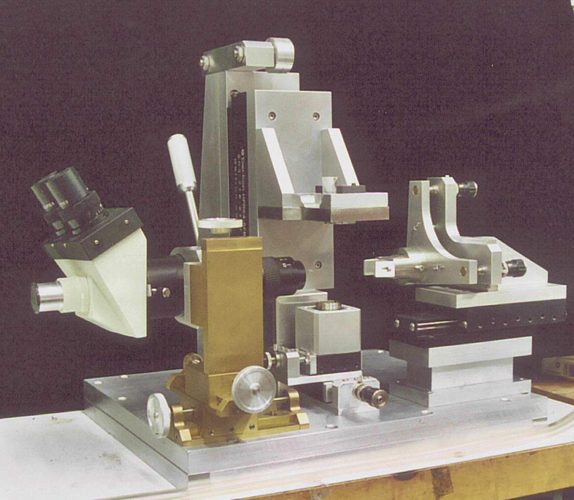
This is the flip-chip bump bonder which was still under construction when I left Rutgers. Precision
linear bearings and differential adjuster screws were used to obtain
accurate alignment and control needed for bump bonding.